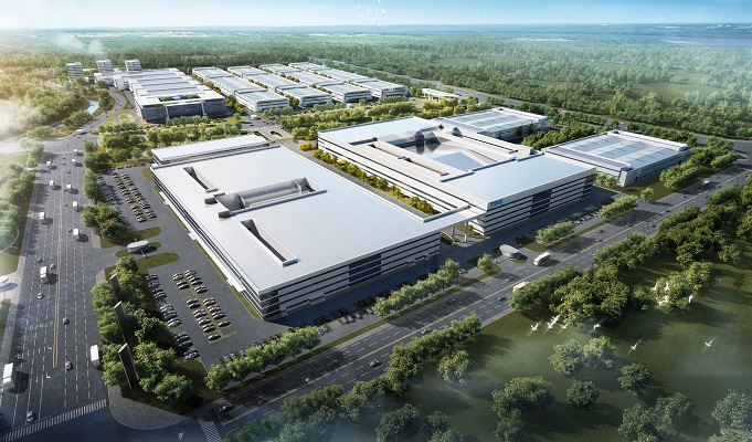
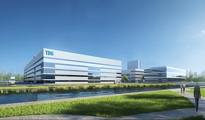
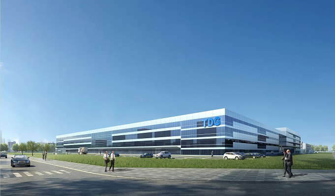
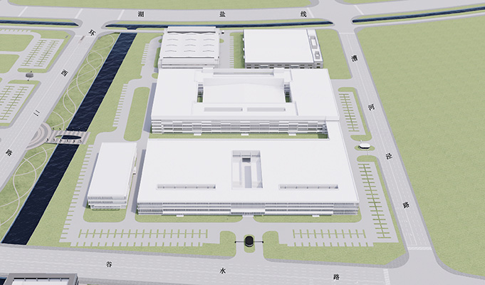
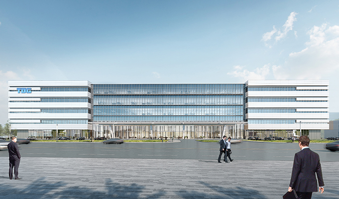
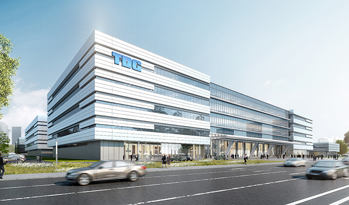
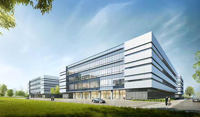
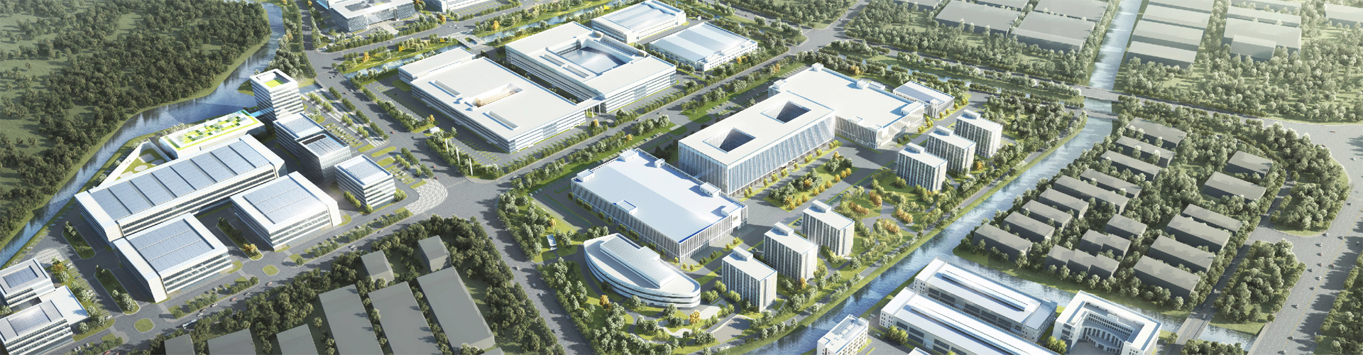
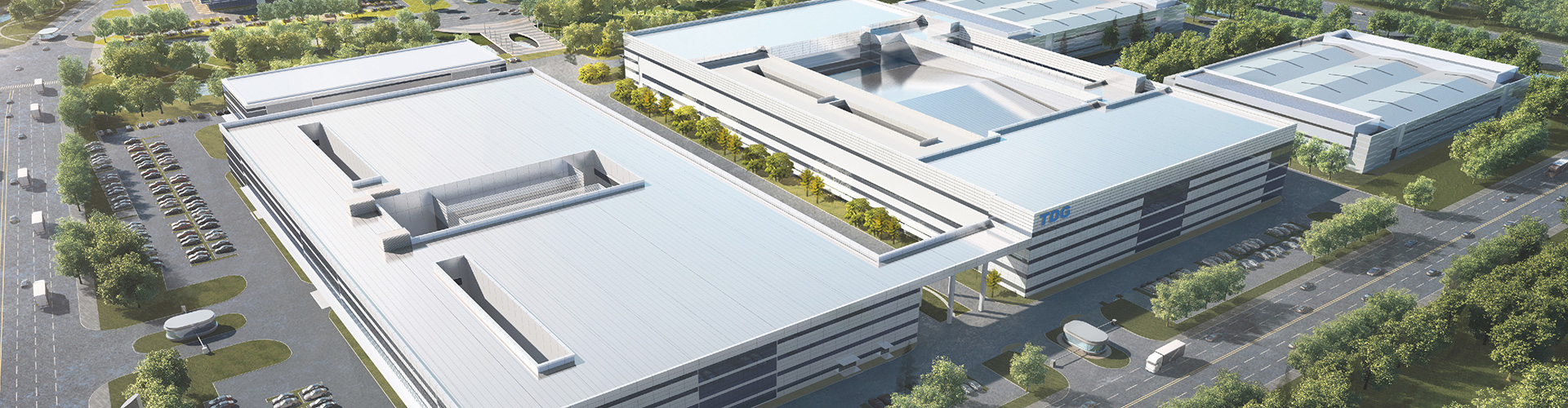
中文

Positioning of Haining Pan-semiconductor TDG Park

It is aimed to industry related to equipment that support core semiconductors’ development, auxiliary materials and the third generation semiconductor materials and devices, core RF devices and modules, magnetic components and modules, ceramic substrates, etc.Committed to building a pan-semiconductor industry ecological chain and building the country's first p...

Overview of the Park

TDG Park I

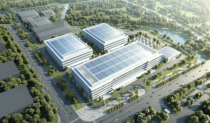
As an important carrier of the Haining Pan-Semiconductor Industrial Park, the planning of Tiantong Phase I Park and Tiantong Phase II Park is based on the third-generation semiconductor materials and devices, core RF devices and modules, magnetic components and modules, ceramic substrates, and semiconductor-related Manufacturing equipment and other industries form a comprehensive pan-semiconductor R & D, manufacturing, sales, and service specialized industrial base.
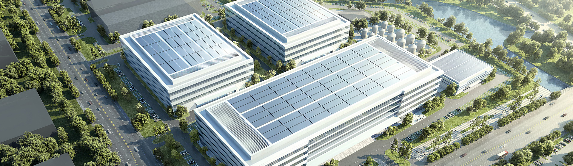
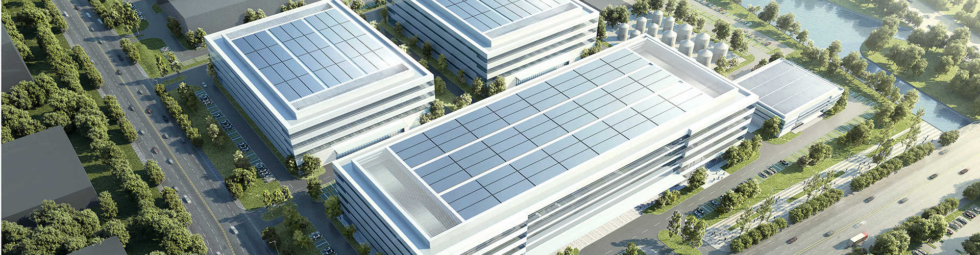
145 mu

Total area

11 10,000 square meters

Total surface area

30 100 million yuan

Park project total investment

50 100 million

Total annual output value after the project reaches capacity

TDG Park II

Tiantong Phase II covers an area of about 207 acres, with a total building area of about 230,000 square meters. The commercial service center covers an area of 40.7 acres, and the industrialized service center covers an area of 165.9 acres. The park plans to introduce third-generation semiconductor materials and devices, core RF devices and modules, magnetic components and modules, ceramic substrates, and semiconductor-related manufacturing equipment.

207 mu

Total area

23 10,000 square meters

Total surface area

40.7 mu

Commercial Service Center Area

165.9 mu

Occupation of industrial service center

Enterprise Services

news center